Showing posts with label Programming. Show all posts

Sunday, March 4, 2018

M5Stack LoRa Range Improvement


Last month I started working on a project to control GPIO pins on a device (relatively) very far away using LoRa technology. Most of the showstopper problems seem to have been resolved. Well, at least getting the RadioHead code working on the M5Stack. This blog entry continues on that topic...

TL;DR
  • VisualMicro Arduino projects in Visual Studio, using 32u4 (see also Adafruit 32u4) and M5Stack - both over LoRa.
  • M5Stack RSSI is a solid RSSI strength of 10 points worse than the exact same code on 32u4 which has the exact same RA-02 AI-Thinker LoRa device.
  • Recall from previous blog, LoRa RST and IRQ are reversed. (RST is actually GPIO36 input only; unusable). Otherwise it would have been: Beep = LoRa reset. 
  • M5Stack Speaker (GPIO25) is shared with LoRa Interrupt. (beep = interrupt?)
  • The M5Stack display shares the NSS pin with the LoRa module. (poke registers with care!)
  • The receiver and transmitter need to be configured EXACTLY the same for best range (more than just the same frequency); but this was not the problem with our poor RSSI
  • My LoRa-GPIO project and required RadioHead and M5Stack libraries merged to master on GitHub
  • When updating library (include) code, Visual Studio apparently does not look at file dates and may use previous compiled code; clean project after library changes.
The latest working (although not very pretty) Very Remote Lora-GPIO Control and Monitoring Project code has been merged onto my master branch.

I've merged my M5Stack development branch back to my RadioHead master branch. This was a "Squash and Merge". Normally I like to keep the history... but as the RadioHead owners prefer a single patch file, perhaps this will be better. Time will tell. History is still in the branch.

I've submitted a PR to Adafruit at their request, as well as well as sent a patch file to Mike at ReadioHead. Ok, this is weekend and evening working, certainly not some of my best polished work. I need to go back and clean things up.

My M5Stack library fork is, and has been up to date on the master branch. (no branches)

The main LoRa-GPIO solution contains several projects as noted in the GitHub readme. These are all Arduino-style projects using the really awesome VisualMicro add-in for Visual Studio.

As a side note, while working on this - I found what appears to be GitHub branch-to-branch compares not working properly.  (if it *does* work properly and I'm simply not doing it correctly, please let me know)

I've been reading through the ARRL Ham Radio License manual. I don't know if I will actually get a ham license, but wow - what a great book this is to cover the essentials of what you need to know for RF communications (such as the LoRa for this project). Although I had a ton of classes in college covering a wide variety of electronics, electromagnetism, communications, even an entire class on antenna theory... this ARRL book contains a lot of relatively straightforward, every-day language on the practical essentials of radio frequency communication - all in one place. The ARRL web site also has some excellent resources. Ok, there's also pretty much NO math, NO theory: Just useful facts. So this is certainly not a book for how or why or how to apply to new problem. Still, it is a quite good book. Highly recommended & would make a great gift for someone new to the field.

So on to the testing... now that I have the RadioHead drivers working, I actually went back to the M5Stack example code (Sandeep drivers renamed M5LoRa). Recall that I have the RadioHead drivers on a remote 32u4 sending LoRa packets. Here's the sample code for the M5Stack receiver (Arduino: File - Examples - M5Stack - Modules - LoRa - LoRaReceiver) :


#include 
#include 

#define LORA_CS_PIN   5
#define LORA_RST_PIN  26
#define LORA_IRQ_PIN  36

void setup() {
  
  M5.begin();

  // override the default CS, reset, and IRQ pins (optional)
  LoRa.setPins(LORA_CS_PIN, LORA_RST_PIN, LORA_IRQ_PIN); // set CS, reset, IRQ pin
  Serial.println("LoRa Receiver");
  M5.Lcd.println("LoRa Receiver");

  // frequency in Hz (433E6, 866E6, 915E6)
  if (!LoRa.begin(433E6)) {
    Serial.println("Starting LoRa failed!");
    M5.Lcd.println("Starting LoRa failed!");
    while (1);
  }

  // LoRa.setSyncWord(0x69);
  Serial.println("LoRa init succeeded.");
  M5.Lcd.println("LoRa init succeeded.");
}

void loop() {
  // try to parse packet
  int packetSize = LoRa.parsePacket();
  if (packetSize) {
    // received a packet
    Serial.print("Received packet: \"");
    M5.Lcd.print("Received packet: \"");

    // read packet
    while (LoRa.available()) {
      char ch = (char)LoRa.read();
      Serial.print(ch);
      M5.Lcd.print(ch);
    }

    // print RSSI of packet
    Serial.print("\" with RSSI ");
    Serial.println(LoRa.packetRssi());
    M5.Lcd.print("\" with RSSI ");
    M5.Lcd.println(LoRa.packetRssi());
  }
}

This code writes to  both the M5Stack display as well as the serial port. The display is cool as I don't need to remember to disconnect the serial port when reprogramming. HOWEVER: You may recall from my previous blog that the M5Stack display *and* LoRa module share the NSS (slave select) pin. That simply sounds dangerous (and indeed I observed some display oddities), so I put M5Stack LoRa to sleep when writing to the display.

The shocking thing here is that there's up to a difference of TEN in RSSI values as compared to using the RadioHead drivers. (RSSI 36 vs 26). As this is a log scale, that's a 10x difference in power! Now - this is not to say that the Sandeep library has a problem just because it is polling rather than using interrupts. It is a matter of default configuration. I picked apart the RadioHead control register libraries and added a note about the matching importance:


When printing the register values from the Sandeep (M5LoRa) library, (move the readRegister from the private to public section)...

    Serial.print("0x");
    Serial.print(LoRa.readRegister((uint8_t )0x1d),HEX);
    Serial.print(", 0x");
    Serial.print(LoRa.readRegister((uint8_t )0x1e),HEX);
    Serial.print(", 0x");
    Serial.print(LoRa.readRegister((uint8_t )0x26),HEX);


There's a SINGLE BIT different (CRC not enabled!):  0x72, 0x70, 0x4 - alas that didn't seem to make much of a substantial difference in RSSI values. I supposed I had expected different error coding, spreading factor, or some other obvious difference.

I confirmed the running values of RadioHead cinfig registers are also 0x72, 0x70, 0x4 - but the RSSI is typically -25 whereas the Sandeep (M5Lora) drivers report an RSSI of typically -35!

So the next thing is: how to each of them calculate RSSI?


Well, the Sandeep / M5Lora library does this:

int LoRaClass::packetRssi()
{
  return (readRegister(REG_PKT_RSSI_VALUE) - (_frequency < 868E6 ? 164 : 157));
}

float LoRaClass::packetSnr()
{
  return ((int8_t)readRegister(REG_PKT_SNR_VALUE)) * 0.25;
}

But the RadioHead library does this:
// Remember the last signal to noise ratio, LORA mode
// Per page 111, SX1276/77/78/79 datasheet
_lastSNR = (int8_t)spiRead(RH_RF95_REG_19_PKT_SNR_VALUE) / 4;

// Remember the RSSI of this packet, LORA mode
// this is according to the doc, but is it really correct?
// weakest receiveable signals are reported RSSI at about -66
_lastRssi = spiRead(RH_RF95_REG_1A_PKT_RSSI_VALUE);
// Adjust the RSSI, datasheet page 87
if (_lastSNR < 0)
 _lastRssi = _lastRssi + _lastSNR;
else
 _lastRssi = (int)_lastRssi * 16 / 15;
if (_usingHFport)
 _lastRssi -= 157;
else
 _lastRssi -= 164;


Grr... So ok, the difference in RSSI appears to be simply a different calculation.  The real test is: how far away can the units be and still communicate? I'm still happy I have the RadioHead libraries working. In my opinion is is clearly the superior code.

So reference check: after all the code changes, let's try same units: 32u4 to 32u4. Cleaned project, full rebuild. RSSI value is -19 or -20! Rechecking the M5Stack, RSSI is -27.  So even with the same codebase and same calcs, the M5Stack LoRa has a poorer RSSI value. Using an external battery power source and the value improves to RSSI = -24.

So, as mentioned about - I've been reading about real world antennas, so perhaps the M5Stack antenna has an issue. Well, I tried that as well, replacing the internal antenna with one of those external antennas - identical to the one on the 32u4. Still there's a discrepancy in RSSI values between the two devices.

What else? Ok, so there's a speaker in the M5Stack. Poking around with that, defined in:

libraries\M5Stack\src\utility\Config.h

there's a declaration:

// BEEP PIN
#define SPEAKER_PIN 25

Ah yes, GPIO25, our friend. The LoRa interrupt pin.  (sigh)

So perhaps all the extras in the M5Stack are indeed causing a problem. I tried to disable a few things  such as the speaker init, but no luck. I do however, have another Console (without display) app that is specifically targeted for the 32u4, but with the magic of simply changing platforms in the IDE, can be recompiled and sent to the M5Stack!  RSSI about that same at -27 (ranging from -23 to -29).  Replace with the exact same code on the 32u4 and the RSSI is a full 10 points better at -17.  (10x improvement in signal strength!).

I tried another M5Stack unit with a different LoRa module. Same result.

So at this point, I really believe it is a hardware issue. I've been unable to get a copy of the schematic for the M5Stack LoRa module, However the 32u4 has a pin connection diagram here.

As soon as hardware is questioned - the first thing to do is of course add some capacitors! I added a 10uF and a 10pf cap directly to the power input to the RA-02.


In the pic, you can see I fished a new, external antenna along with the new caps. And ya, I got a little close to the side of the M5 Lora module.

Additionally I added a shield (aluminum foil sandwiched between two layers of clear packing tape) to both sides of the LoRa module. After all - there is an ESP32 microprocessor buzzing away just on the other side of the PCB!


The first field test was a relative success! I more than doubled the original range! Ok, so I didn't actually test after each change, so I don't know exactly which was the most effective in extending the range.

Note the Semtech site has a bunch of LoRa resources, including this cool LoRa calculator (I will include in my GitHub repository in the docs container, in case the link to Semtech ever breaks.


Note that I am currently transmitting at 125kHz. Lowering this increases range! Lower this to about 15.6kHz and you get another 10db in "link performance". (in theory).

Overall I am quite happy with the result. Ok, I'm not seeing multi-kilometer ranges. But that's also line-of-sight. My transmitter is on the kitchen table - with the entire garage between it and the M5Stack receiver. Next test will be from line of site.

The super exciting thing is I have a prototype from the kind folks at M5Stack arriving in the mail soon for the next potential version of the LoRa module. I am quite interested in seeing how well it performs.

Stay tuned for my next blog where I work on the prototype V2 LoRa modules with its own embedded ATMEGA328.


Resources, Inspiration, Credits, and Other Links:


Saturday, February 3, 2018

First FPGA Test Drive with Altera Cyclone IV

I decided to finally learn how to program an FPGA! Here are some first impressions and notes to self for future reference.


TL;DR

  • Blaster drivers need to be manually installed from C:\intelFPGA_lite\17.1\quartus\drivers
  • Cyclone IV board is EP4CE6E22C8; do not use default "auto device" (for Pin Planner) 
  • Verilog file added manually, module name must match file name and is case sensitive
  • Source files in the project are "Design Entities"
  • Do not insert to remove the USB Blaster ribbon cable while the device is powered on.
  • Download vendor board files here
  • JTAG programming of FPGA is temporary and lost upon power cycle

I ordered my first FPGA board - the Altera Cyclone IV EP4CE6 FPGA Development Kit and USB Blaster from the Numon Electric Cyberport Store on Aliexpress thanks to inspiration by Amitesh. He did all the footwork to find what seems to be the coolest Cyclone FPGA board that can still be programmed with the free version software. (note the really cool GX version with Nios processor needs software costing thousands of dollars)

If you order the board from Numon Electric, they have a download available on one-drive that includes a ton of really great documentation, sample code, and more. The file is called "RZ301 EP4CE6 development board.zip" however the contents of that zip file consist of mainly a single file "Altera Cyclone IV board V3.0.rar". Windows users will be annoyed that there's no native tool to easily extract RAR files. Having a linux VM or WSL will be handy here. The latest version of winzip also appears to now support RAR extraction.

Overall I was quite happy with the responsive customer service, prompt delivery, and quality of my new FPGA board. If you look close at the picture of my board, the actual silkscreen quality is much better than shown: the blur is from the poor picture.

While awaiting delivery of my Cyclone, I found this other tiny, inexpensive FPGA created by Luke Valenty. Note that if you order on the tinyfpga store web site, you can pay with Amazon, without having the hassle of creating an account, etc. This board is so cool, I think I will have a separate blog about it later.

Surprisingly, my Cyclone board arrived relatively quickly in only about 2 weeks! (the estimate at order time was 19 to 39 days)

In order to program the Cyclone board, the Altera Quartus Prime Lite software is needed. Unlike some other programs, installation was quick and easy.

IMPORTANT: Do not insert to remove the USB Blaster ribbon cable while the device is powered on. There was an included warning that the board would likely be damaged. I did not test this.

The USB Blaster was not Plug-N-Play, and Quartus Prime did not see it:


A quick google search indicated that the drivers need to be manually installed; instructions copied from Altera site here for reference:
The Altera On-Board USB-Blaster II cable appears as Altera USB-Blaster (unconfigured) when first attached to your system. After it has been configured by the Quartus Prime software, it will appear as Altera USB-Blaster II (JTAG interface) and then Altera USB-Blaster II (SystemConsole interface). You might need to install drivers for each of these interfaces; follow the steps below to install the drivers.

You must have system administration (Administrator) privileges to install the USB-Blaster and USB-Blaster II download cable driver.

Driver Installation for Altera USB-Blaster

  1. Plug the USB-Blaster download cable into your PC. The Found New Hardware dialog box appears.
  2. Select Locate and install driver software (recommended).
  3. Select Don't search online.
  4. When you are prompted to Insert the disc that came with your USB-Blaster, select I don’t have the disc. Show me other options.
  5. Select Browse my computer for driver software (advanced) when you see the Windows couldn’t find driver software for your device dialog box.
  6. Click Browse, and browse to the <Path to Quartus Prime installation>\drivers\usb-blaster directory.
    • Note: Do not select the x32 or x64 directories.
  7. Click OK.
  8. Select the Include subfolders option, and click Next.
  9. If you are prompted Windows can’t verify the publisher of this driver software, select Install this driver software anyway in the Window Security dialog box. The installation wizard guides you through the installation process.
  10. When The software for this device has been successfully installed dialog box appears, click Close.
  11. To complete your installation, set up programming hardware in the Quartus Prime software.

Driver Installation for Altera USB-Blaster II

  1. Plug the USB-Blaster II cable into your PC.
  2. Open the Device Manager, and right-click on the Unknown device under the Other devices branch.
  3. Select Update Driver Software.
  4. Select Browse my computer for driver software.
  5. Enter the location of the Quartus Prime software USB-Blaster II driver files directory (<Path to Quartus Prime installation>\drivers\usb-blaster-ii) in the Search for driver software in this location field.
  6. Click Next.
  7. Click Install in the Would you like to install this device software? Windows security dialog box.
  8. Close the Update Driver Software - Altera USB-Blaster II (Unconfigured) successful installation notification. The Device Manager now shows a new branch called JTAG cables with an Altera USB-Blaster II (Unconfigured) node.
  9. Open the Quartus Prime Programmer. Within a few seconds, the JTAG cables branch displays two nodes: Altera USB-Blaster II (JTAG interface) and Altera-USB Blaster II (System Console interface).

The pin-out of the USB Blaster cable is such that it can be used for three different programming modes: AS, PS and JTAG, as shown in this pin definition table from the Intel FPGA USB Download Cable User Guide:


The important thing to note here is that programming via JTAG is temporary! My board came pre-programmed with something that cycles though the 4 LED's on the board. There's always a little fear of sending a new program that toasts your new FPGA (yes, this is absolutely possible!). So it is cool that upon power cycle, the original config is loaded back into the FPGA to confirm all us well. Fortunately my first program actually worked the very first time!

As with all development environments, Quartus has its own annoyances. I found it very difficult to simply: File - Create New Project and get something to actually work without a bit of fussing.

The first annoyance is the default directory. For example, in Visual Studio, the IDE is smart enough to know to actually create a directory for your project. Any you only need to type it once. Here, the default directory is the IDE, and projects are created there unless explicitly stated in THREE places. So the new Project Wizard starts here:


Be sure to append a project name to the directory:


Or better yet, I keep all my project in c:\workspace\ in this case for the new myFPGAgizmo project:


You can set the default location in: Tools - Options - General - Default File Location.

I created an empty project...


and did not add any design files...


This next step is important... the default device is set to "Auto". What this does is completely disables the Pin Planner feature needed later, giving an error:
Cannot display Pin Planner the current Compiler settings assign an AUTO device.
For a newbie like me.. the solution was not very obvious. To avoid this, change the default at new project time to EP4CE6E22C8


The tools are left as default:


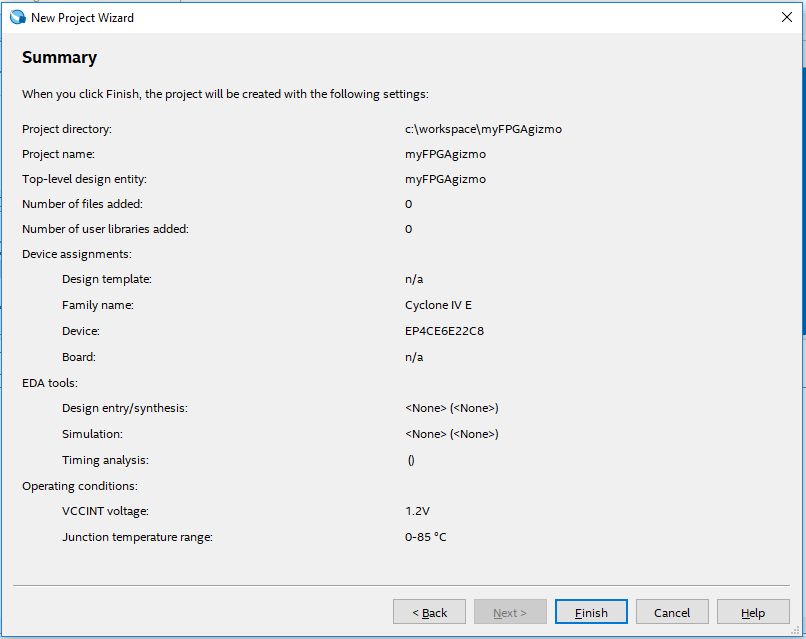
On the final Project Wizard page, the summary is shown:


Tada! All done, right? Nope. The "Wizard" still does not actually complete a project.

Double-click on "myFPGAgizmo" to edit the code, and a nice, less-than-intuitive error pops up:
Can't find design entity "myFPGAgizmo".
Not exactly to most intuitive error message for a newbie. 


Good luck finding "Add Design Entity" in the menu. Here, you just need to know that a new Design File needs to be manually added (why the wizard does not do this, I do not know).

So from what I can tell:  a source "File" == "Design Entity".

File - New - Verilog HDL File:


Quartus does not give you an opportunity to name this file when it is first created. Only at save time will it prompt to give it a new name. Visual Studio users will not be impressed.


Now another important note: The name of the module MUST MATCH the name of the "top level" file name, and it is case sensitive. The "top level design entity" is that file first listed. You just need to know this. Otherwise the Quartus software gives the less-than-intuitive error message:
Top level design entity "myFPGAgizmo" is undefined 
Here the "myFPGAgimoName" needs to be the same as the file name "myFPGAgizmo":


So after dealing with those annoyances the learning curve, I was finally able to write some Verilog that I found in another tutorial (see page 14):


module myFPGAgizmo (x1, x2, f); 
  input x1, x2; 
  output f; 
  assign f = (x1 & ~x2)|(~x1 & x2); 
endmodule 


This is where things get interesting. It is one thing to write some code, but getting it to interface to the real world is what makes it fun! Normally I/O is abstracted through complex device drivers and API calls. However, it does not get much more direct in FPGA programming, as the actual pins on the chip are assigned to variables in our code! Even better, there's no bizarre renumbering that I find ridiculously frustrating in the world of Arduino programming. There's a single pin number. Ahhh. What bliss.


As can be seen in the schematic, Pin 87 is LED4, and Pins 88 and 89 are tied to keys (button switches) KEY1 and KEY2 (but yes, instead labeled S1 and S2 on the board). Yes, those are the actual pins numbers on the Cyclone IV - pins 87, 88, and 89. No big deal, right? Well, sure - but apparently not all engineers agree. Just google "pin numbering arduino" to see how many hours have been lost to frustrating abstracted re-numbering.

Once code is entered, it is compiled using the menu: Processing - Start Compilation. When the pins are not actually assigned, there will be a compiler warning:

Critical Warning (169085): No exact pin location assignment(s) for 3 pins of 3 total pins. For the list of pins please refer to the I/O Assignment Warnings table in the fitter report.
Click on Assignments - Pin Planner. (recall above, we explicitly assigned our chip part number, otherwise this feature is not available).  If you double-click in the Location column, a drop-down list will appear:


We need to assign the pins to keys and LED as shown in the schematic:


Simply close the Pin Planner and compile again. We're ready to send the FPGA code to our device!

Note the USB Blaster connection in the very first picture on this page.

Click Tools - Programmer. If the currently selected hardware says "No Hardware", click the "Hardware Setup" button (make sure your device is plugged inn, and drivers installed)....


In this case, I selected the USB Blaster by double-clicking on it.

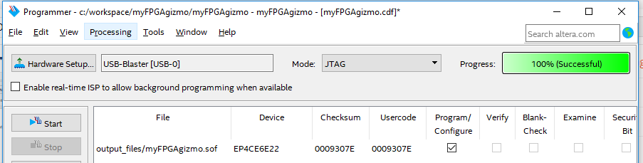
To send the FPGA code to the device, select "Processing - Start" (or simply press the "Start Button"). If successful, there will be an indication in the progress box:


That's it! There's now an XOR gate programmed in the FPGA. Press S1 or S2 to have the LED got out. Press both or leave both unpressed and the LED1 will be illuminated. Cool.

Note we've programmed the FPGA via the JTAG connector on the board. When the board is power cycled, we'll lose these changes and the board will revert back to vendor ship default.


Note that if you find cheap Cyclone boards on flea bay, the most recent version of Quartus does NOT support the older chips! I sadly learned this after buying a cheap, bare-bones Cyclone II and then noticed it was not listed as a device option in the Quartus IDE. The latest version supporting the Cyclone II is Quartus version 13.0sp1 from 2013. (I wonder if side-by-side installs are supported? I didn't try)

Here's a chart of supported devices vs Quartus versions specifically the Cyclone series:


That's it for now... send me a message on twitter if you have any feedback / suggestions / notice any typos.


Resources, Inspiration, Credits, and Other Links:


Find gojimmypi at gojimmypi.github.io

I'm currently working on my new blog home at  gojimmypi.github.io After implementing a variety of features such as dark mode , syntax hi...