
TL;DR
- Blaster drivers need to be manually installed from C:\intelFPGA_lite\17.1\quartus\drivers
- Cyclone IV board is EP4CE6E22C8; do not use default "auto device" (for Pin Planner)
- Verilog file added manually, module name must match file name and is case sensitive
- Source files in the project are "Design Entities"
- Do not insert to remove the USB Blaster ribbon cable while the device is powered on.
- Download vendor board files here
- JTAG programming of FPGA is temporary and lost upon power cycle
I ordered my first FPGA board - the Altera Cyclone IV EP4CE6 FPGA Development Kit and USB Blaster from the Numon Electric Cyberport Store on Aliexpress thanks to inspiration by Amitesh. He did all the footwork to find what seems to be the coolest Cyclone FPGA board that can still be programmed with the free version software. (note the really cool GX version with Nios processor needs software costing thousands of dollars)
If you order the board from Numon Electric, they have a download available on one-drive that includes a ton of really great documentation, sample code, and more. The file is called "RZ301 EP4CE6 development board.zip" however the contents of that zip file consist of mainly a single file "Altera Cyclone IV board V3.0.rar". Windows users will be annoyed that there's no native tool to easily extract RAR files. Having a linux VM or WSL will be handy here. The latest version of winzip also appears to now support RAR extraction.
Overall I was quite happy with the responsive customer service, prompt delivery, and quality of my new FPGA board. If you look close at the picture of my board, the actual silkscreen quality is much better than shown: the blur is from the poor picture.
While awaiting delivery of my Cyclone, I found this other tiny, inexpensive FPGA created by Luke Valenty. Note that if you order on the tinyfpga store web site, you can pay with Amazon, without having the hassle of creating an account, etc. This board is so cool, I think I will have a separate blog about it later.
Surprisingly, my Cyclone board arrived relatively quickly in only about 2 weeks! (the estimate at order time was 19 to 39 days)
In order to program the Cyclone board, the Altera Quartus Prime Lite software is needed. Unlike some other programs, installation was quick and easy.
IMPORTANT: Do not insert to remove the USB Blaster ribbon cable while the device is powered on. There was an included warning that the board would likely be damaged. I did not test this.
The USB Blaster was not Plug-N-Play, and Quartus Prime did not see it:

A quick google search indicated that the drivers need to be manually installed; instructions copied from Altera site here for reference:
The Altera On-Board USB-Blaster II cable appears as Altera USB-Blaster (unconfigured) when first attached to your system. After it has been configured by the Quartus Prime software, it will appear as Altera USB-Blaster II (JTAG interface) and then Altera USB-Blaster II (SystemConsole interface). You might need to install drivers for each of these interfaces; follow the steps below to install the drivers.
You must have system administration (Administrator) privileges to install the USB-Blaster and USB-Blaster II download cable driver.
Driver Installation for Altera USB-Blaster
- Plug the USB-Blaster download cable into your PC. The Found New Hardware dialog box appears.
- Select Locate and install driver software (recommended).
- Select Don't search online.
- When you are prompted to Insert the disc that came with your USB-Blaster, select I don’t have the disc. Show me other options.
- Select Browse my computer for driver software (advanced) when you see the Windows couldn’t find driver software for your device dialog box.
- Click Browse, and browse to the <Path to Quartus Prime installation>\drivers\usb-blaster directory.
- Note: Do not select the x32 or x64 directories.
- Click OK.
- Select the Include subfolders option, and click Next.
- If you are prompted Windows can’t verify the publisher of this driver software, select Install this driver software anyway in the Window Security dialog box. The installation wizard guides you through the installation process.
- When The software for this device has been successfully installed dialog box appears, click Close.
- To complete your installation, set up programming hardware in the Quartus Prime software.
Driver Installation for Altera USB-Blaster II
- Plug the USB-Blaster II cable into your PC.
- Open the Device Manager, and right-click on the Unknown device under the Other devices branch.
- Select Update Driver Software.
- Select Browse my computer for driver software.
- Enter the location of the Quartus Prime software USB-Blaster II driver files directory (<Path to Quartus Prime installation>\drivers\usb-blaster-ii) in the Search for driver software in this location field.
- Click Next.
- Click Install in the Would you like to install this device software? Windows security dialog box.
- Close the Update Driver Software - Altera USB-Blaster II (Unconfigured) successful installation notification. The Device Manager now shows a new branch called JTAG cables with an Altera USB-Blaster II (Unconfigured) node.
- Open the Quartus Prime Programmer. Within a few seconds, the JTAG cables branch displays two nodes: Altera USB-Blaster II (JTAG interface) and Altera-USB Blaster II (System Console interface).
The pin-out of the USB Blaster cable is such that it can be used for three different programming modes: AS, PS and JTAG, as shown in this pin definition table from the Intel FPGA USB Download Cable User Guide:

The important thing to note here is that programming via JTAG is temporary! My board came pre-programmed with something that cycles though the 4 LED's on the board. There's always a little fear of sending a new program that toasts your new FPGA (yes, this is absolutely possible!). So it is cool that upon power cycle, the original config is loaded back into the FPGA to confirm all us well. Fortunately my first program actually worked the very first time!
As with all development environments, Quartus has its own annoyances. I found it very difficult to simply: File - Create New Project and get something to actually work without a bit of fussing.
The first annoyance is the default directory. For example, in Visual Studio, the IDE is smart enough to know to actually create a directory for your project. Any you only need to type it once. Here, the default directory is the IDE, and projects are created there unless explicitly stated in THREE places. So the new Project Wizard starts here:

Be sure to append a project name to the directory:

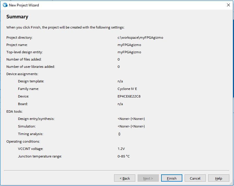
Or better yet, I keep all my project in c:\workspace\ in this case for the new myFPGAgizmo project:

You can set the default location in: Tools - Options - General - Default File Location.
I created an empty project...
and did not add any design files...

This next step is important... the default device is set to "Auto". What this does is completely disables the Pin Planner feature needed later, giving an error:
Cannot display Pin Planner the current Compiler settings assign an AUTO device.For a newbie like me.. the solution was not very obvious. To avoid this, change the default at new project time to EP4CE6E22C8

The tools are left as default:

On the final Project Wizard page, the summary is shown:
Tada! All done, right? Nope. The "Wizard" still does not actually complete a project.
Double-click on "myFPGAgizmo" to edit the code, and a nice, less-than-intuitive error pops up:
Can't find design entity "myFPGAgizmo".
Not exactly to most intuitive error message for a newbie.

Good luck finding "Add Design Entity" in the menu. Here, you just need to know that a new Design File needs to be manually added (why the wizard does not do this, I do not know).
So from what I can tell: a source "File" == "Design Entity".
File - New - Verilog HDL File:

Quartus does not give you an opportunity to name this file when it is first created. Only at save time will it prompt to give it a new name. Visual Studio users will not be impressed.

Now another important note: The name of the module MUST MATCH the name of the "top level" file name, and it is case sensitive. The "top level design entity" is that file first listed. You just need to know this. Otherwise the Quartus software gives the less-than-intuitive error message:
Top level design entity "myFPGAgizmo" is undefined
Here the "myFPGAgimoName" needs to be the same as the file name "myFPGAgizmo":

module myFPGAgizmo (x1, x2, f);
  input x1, x2;
  output f;
  assign f = (x1 & ~x2)|(~x1 & x2);
endmodule
This is where things get interesting. It is one thing to write some code, but getting it to interface to the real world is what makes it fun! Normally I/O is abstracted through complex device drivers and API calls. However, it does not get much more direct in FPGA programming, as the actual pins on the chip are assigned to variables in our code! Even better, there's no bizarre renumbering that I find ridiculously frustrating in the world of Arduino programming. There's a single pin number. Ahhh. What bliss.

As can be seen in the schematic, Pin 87 is LED4, and Pins 88 and 89 are tied to keys (button switches) KEY1 and KEY2 (but yes, instead labeled S1 and S2 on the board). Yes, those are the actual pins numbers on the Cyclone IV - pins 87, 88, and 89. No big deal, right? Well, sure - but apparently not all engineers agree. Just google "pin numbering arduino" to see how many hours have been lost to frustrating abstracted re-numbering.
Once code is entered, it is compiled using the menu: Processing - Start Compilation. When the pins are not actually assigned, there will be a compiler warning:
Critical Warning (169085): No exact pin location assignment(s) for 3 pins of 3 total pins. For the list of pins please refer to the I/O Assignment Warnings table in the fitter report.
Click on Assignments - Pin Planner. (recall above, we explicitly assigned our chip part number, otherwise this feature is not available). If you double-click in the Location column, a drop-down list will appear:

We need to assign the pins to keys and LED as shown in the schematic:

Simply close the Pin Planner and compile again. We're ready to send the FPGA code to our device!
Note the USB Blaster connection in the very first picture on this page.
Click Tools - Programmer. If the currently selected hardware says "No Hardware", click the "Hardware Setup" button (make sure your device is plugged inn, and drivers installed)....

In this case, I selected the USB Blaster by double-clicking on it.
To send the FPGA code to the device, select "Processing - Start" (or simply press the "Start Button"). If successful, there will be an indication in the progress box:
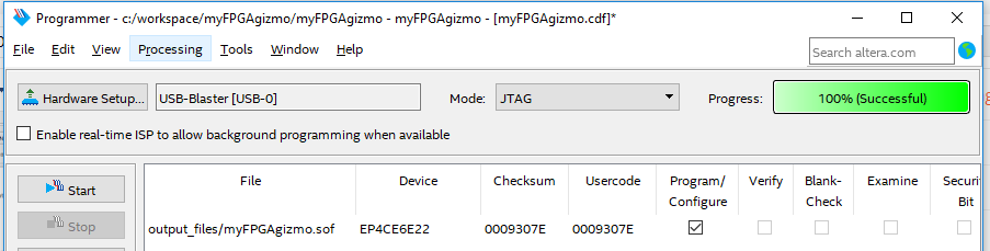
That's it! There's now an XOR gate programmed in the FPGA. Press S1 or S2 to have the LED got out. Press both or leave both unpressed and the LED1 will be illuminated. Cool.
Note we've programmed the FPGA via the JTAG connector on the board. When the board is power cycled, we'll lose these changes and the board will revert back to vendor ship default.
Note that if you find cheap Cyclone boards on flea bay, the most recent version of Quartus does NOT support the older chips! I sadly learned this after buying a cheap, bare-bones Cyclone II and then noticed it was not listed as a device option in the Quartus IDE. The latest version supporting the Cyclone II is Quartus version 13.0sp1 from 2013. (I wonder if side-by-side installs are supported? I didn't try)
Here's a chart of supported devices vs Quartus versions specifically the Cyclone series:

That's it for now... send me a message on twitter if you have any feedback / suggestions / notice any typos.
Resources, Inspiration, Credits, and Other Links:
- Altera - My First FPGA Design Tutorial
- Quartus Prime Introduction Using verilog Designs
- UDemy - Learn VHDL and FPGA Development
- UDemy - FPGA Turbo Series - Implementing a UART
- Verilog HDL support for VSCode
- Verilog Tutorials and Examples at nandland
- Altera Cyclone IV from Numon Electronic Cyberport Store
- Resource file with documentation and samples
- Intel FPGA USB Download Cable User Guide
- Quartus Prime Download
- Altera Device Downloads
- Gnarly Grey UPDuino v1.0 Board
- A Look at TinyFPGA Boards
- UART, Serial Port, RS-232 Interface Code in both VHDL and Verilog for FPGA Implementation
- Altera-Lime Connectivity and DUC/DDC Design Example


Do you have a qsf file for ALL the pins?
ReplyDeleteI know there is a table, but would rather not type them all in if it already exists.
hm. curious. You know... I didn't type those; the file was apparently auto-generated.
ReplyDeleteI'm finding that when I want to change the Location in the Pin Planner that the suggested pins in the drop down lists are completely wrong. For example, pin 87 (led1 according to "Development board pin information.xls" claims to be "DIFFIO_R7p,DEV_CLRn" or something. It would be a lot nicer if the list actually said "PIN_87 LED1".
ReplyDeleteGreat quick start guide, it happens as You said.... Best regards (using Quartus Prime 20.1)
ReplyDeleteThere are example code of this board. I am just get one.
ReplyDeleteI can't seem to download the examples from the one drive website listed above. Is there an alternate download location?
ReplyDeleteI am not aware of an alternate site for the one drive samples. The file is about 280MB. I still have it. I'm happy to get you a copy, but I don't have any practical means for sending something that large. You can send me an email using my blogspot name at gmail.
DeleteHi there Jimmy,
DeleteCould make a MEGA.nz share or Google Drive or One Drive share, and in there put the associated resources (files) for this board?
It looks quite lucrative :)
Go ahead and send me a message at Gmail.
Delete